Documents for programming a microcontroller
In embedded programming, documents have a very important role as they are the main reference sources for developers to know how the processor works and how to configure it. Those documents mainly come from the processor manufacture, including example Board Schematic, the Datasheet, Programming Manual, and the most important Reference Manual with details of the target microprocessor.
Last update: 2022-05-10
Table of Content
Datasheet (Product Specifications)#
This document contains highlight of the target microprocessor with main features and capabilities. Many people are confused with Reference Manual, but when comparing the content, they are written for different purpose. This document is helpful when designing a PCB. It gives recommended layout for things like signal characteristic, NRST pin, ADC pins, Boot mode, etc.
Datasheet provides the following:
- General description including product line, speed, memory, operating voltage, temperature range
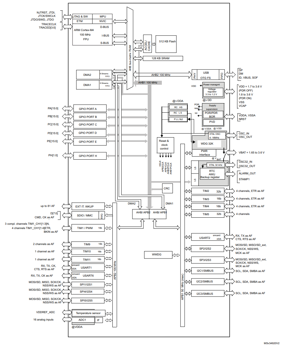
- Device overview with block diagram, available peripherals and functions
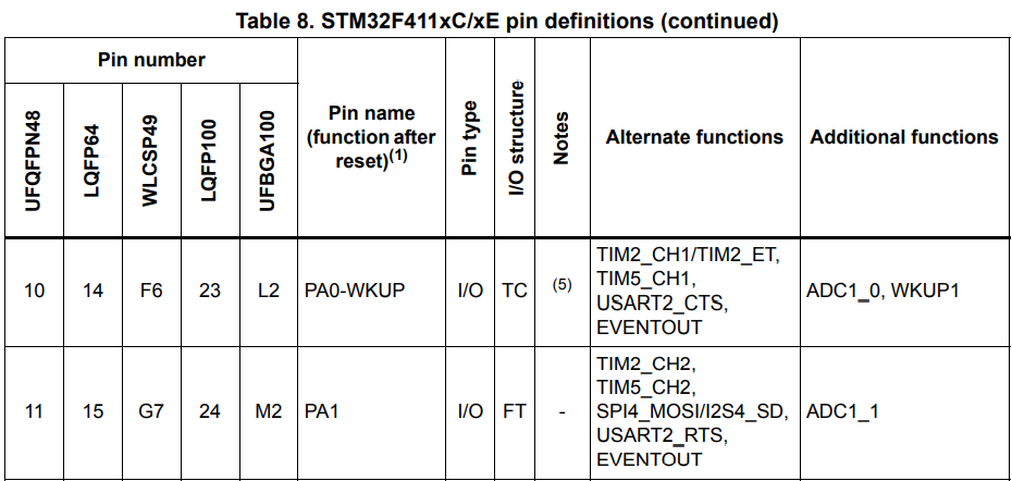
- Pinouts and pin descriptions
- Memory map and memory ranges
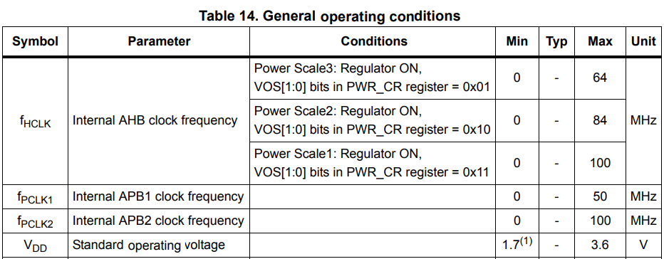
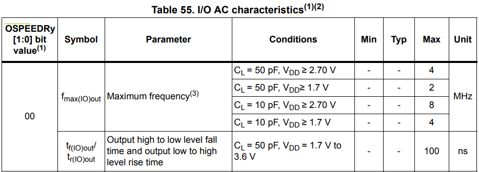
- Electrical Characteristics
- Package information, for modeling PCB footprints
- Ordering Information
Excerpt from DS10314 — STM32F411xC STM32F411xE Datasheet
Boot modes
At startup, the boot pin and boot selector option bit are used to select one of the three boot options:
- boot from User Flash memory
- boot from System Memory
- boot from embedded SRAM
The bootloader is located in system memory. It is used to reprogram the Flash memory by using USART1(PA9/10), USART2(PD⅚), USB OTG FS in device mode (PA11/12) through DFU (device firmware upgrade), I2C1(PB6/7), I2C2(PB10/3), I2C3(PA8/PB4), SPI1(PA⅘/6/7), SPI2(PB12/13/14/15) or SPI3(PA15, PC10/11/12).
For more detailed information on the bootloader, refer to Application Note: AN2606, STM32 microcontroller system memory boot mode.
Pinout table
I/O structure with marker FT for 5 V-tolerant I/O, TT or TC for 3.3 V-only I/O.
Unless otherwise specified by a note, all I/Os are set as floating inputs during and after reset.

Reference Manual#
This is by far the most important document in order to program the target device. It defines all information about the core and peripheral at register level with bit-by-bit description. By using only this document, developer still can program the chip without any higher level API — usually called Bare-metal/Register-based programming.
Reference Manual provides the following:
- System Architecture with bus, peripherals, and connections
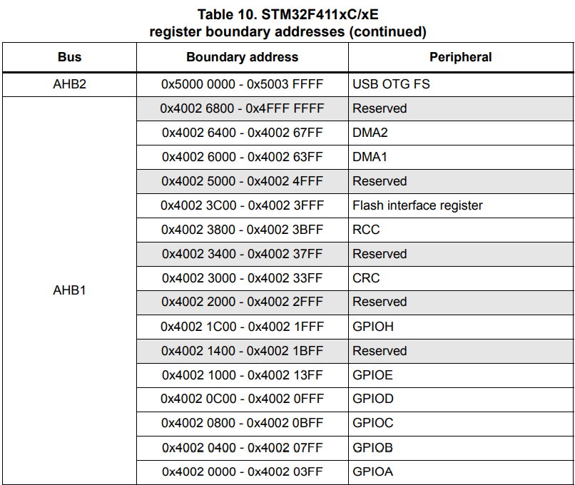
- Memory map and boundary address
- Boot configuration and vector table relocation
- Peripheral with details features, descriptions, and structure
- Register name and bit-fields for all accessible registers
- Code examples using CMSIS header files
Excerpt from RM0383 — STM32F411xC/E advanced Arm®-based 32-bit MCUs

Boot configuration
The boot mode configuration is latched on the 4th rising edge of SYSCLK after a reset, and is also re-sampled when exiting from Standby mode. After this startup delay has elapsed, the CPU always fetches the top-of-stack value from address 0x00000000, then starts code execution from the boot memory at 0x00000004.
Depending on the selected boot mode, main Flash memory, system memory or SRAM is accessible as follows:
-
Boot from main Flash memory: the main Flash memory is aliased in the boot memory space
0x00000000, but still accessible from its original memory space0x08000000. -
Boot from system memory: the system memory is aliased in the boot memory space
0x00000000, but still accessible from its original memory space0x1FFF0000. -
Boot from the embedded SRAM: the SRAM is aliased in the boot memory space
0x00000000, but it is still accessible from its original memory space0x20000000.
Physical remap
For application code which is located in a different address than 0x08000000, some additional code must be added in order to be able to serve the application interrupts. A solution will be to relocate by software the vector table to the internal SRAM, at the initialization phase:
- Copy the vector table from the Flash (mapped at the base of the application load address) to the base address of the SRAM at
0x20000000 - Remap SRAM at address
0x00000000, usingSYSCFGconfiguration register 1
Embedded bootloader
The embedded bootloader mode is used to reprogram the Flash memory using one of the following serial interfaces:
- USART1 (PA9/PA10)
- USART2 (PD5/PD6)
- I2C1 (PB6/PB7)
- I2C2 (PB10/PB3)
- I2C3 (PA8/PB4)
- SPI1 (PA4/PA5/PA6/PA7)
- SPI2 (PB12/PB13/PB14/PB15)
- SPI3 (PA15/PC10/PC11/PC12)
- USB OTG FS (PA11/12) in Device mode (DFU: device firmware upgrade).
The USART peripherals operate at the internal 16 MHz oscillator (HSI) frequency, while the USB OTG FS require an external clock (HSE) multiple of 1 MHz (ranging from 4 to 26 MHz).
The embedded bootloader code is located in system memory. It is programmed by ST during production.
Debug pin
During and just after reset, the alternate functions are not active and most of the I/O ports are configured in input floating mode, except the debug pins are in AF pull-up/pull-down mode immediately:
- PA15: JTDI in pull-up
- PA14: JTCK/SWCLK in pull-down
- PA13: JTMS/SWDAT in pull-up
- PB4: NJTRST in pull-up
- PB3: JTDO in floating state
Programming Manual#
This programming manual provides information for application and system-level software developers. It gives a full description of the STM32 Cortex™-M0 processor programming model, instruction set and core peripherals.
Programming Manual provides the following:
- Processor Modes, Stacks
- Memory model
- Exception model, the Vector table and the interrupt service routines
- Fault handling
- Power management: enter Sleep mode, Wake up
- The Instruction Set
- CMSIS intrinsic functions
- Core Peripherals:
- Memory Protection Unit (MPU)
- Nested vectored interrupt controller (NVIC)
- System control block (SCB)
- SysTick timer (STK)
Excerpt from PM0214 — STM32 Cortex®-M4 MCUs and MPUs programming manual
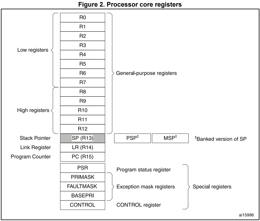
Processor modes
Thread mode: Used to execute application software. The processor enters Thread mode when it comes out of reset
Handler mode: Used to handle exceptions. The processor returns to Thread mode when it has finished exception processing.
Stacks
The processor uses a full descending stack. This means the stack pointer indicates the last stacked item on the stack memory.
The processor implements two stacks, with independent copies of the stack pointer:
- The main stack and
- The process stack
In Thread mode, the CONTROL register controls whether the processor uses the main stack or the process stack:
0: Main Stack Pointer (MSP)(reset value). On reset, the processor loads the MSP with the value from address0x00000000.1: Process Stack Pointer (PSP).
In Handler mode, the processor always uses the main stack.
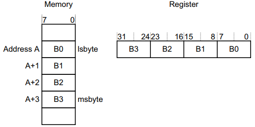
Memory endianness
The processor views memory in little-endian format. It stores the least significant byte (lsbyte) of a word at the lowest-numbered byte, and the most significant byte (msbyte) at the highest-numbered byte.
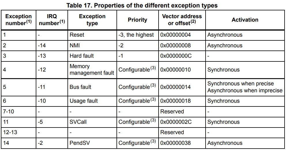
Vector table
On system reset, the vector table is fixed at address 0x00000000. The least-significant bit of each vector must be 1, indicating that the exception handler is Thumb code.
Application Note#
There many Application Note documents provided by ST. Each document present the usage, design, and advice for a specific application or feature.
Application Note provides the following:
- Peripherals architecture in hardware and software
- Operation characteristic
Excerpt from AN4031 — Using the STM32F2, STM32F4 and STM32F7 Series DMA controller
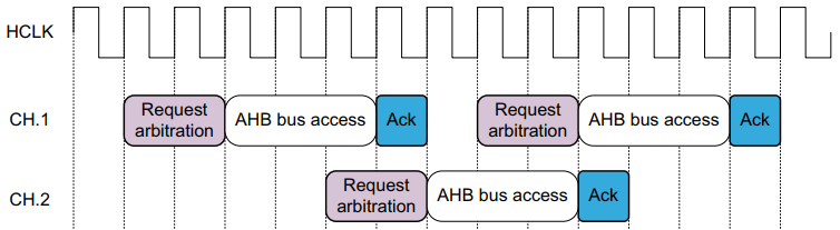
DMA transfer timing
For the case where only one DMA channel is active, a new hardware back-to-back request can not be handled by the DMA before the completion of the previous one, adding one AHB clock cycle for the final idle phase of the DMA request-acknowledge handshake protocol.
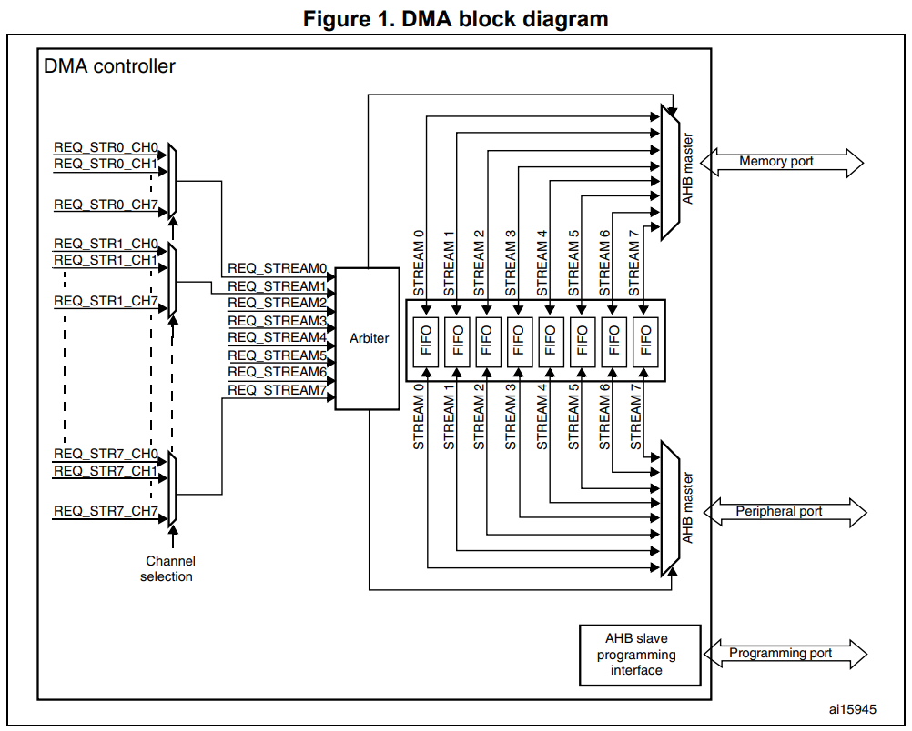
When more than one channel is requesting a DMA transfer, the DMA request arbitration can be performed meanwhile the two last cycles of when the AHB bus is accessed by the DMA. Request arbitration overhead is then masked by the AHB bus transfer time.
In case not only two channels, but two DMA controllers are used (in products that offer this possibility), two DMA transfers can be processed in parallel, as long as they are not conflicting within the bus matrix, not accessing the same slave device.
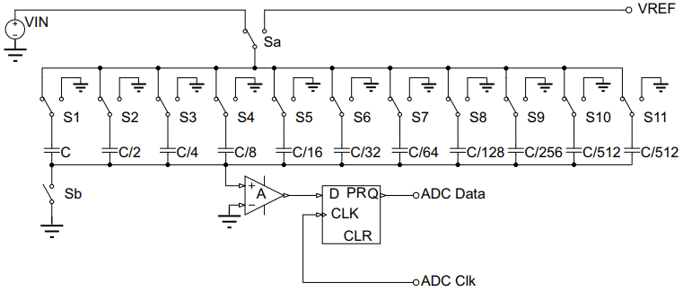
Excerpt from AN2834 — How to get the best ADC accuracy in STM32 microcontrollers
SAR ADC internal structure
The ADC embedded in STM32 microcontrollers uses the SAR (successive approximation register) principle, by which the conversion is performed in several steps. The number of conversion steps is equal to the number of bits in the ADC converter. Each step is driven by the ADC clock. Each ADC clock produces one bit from result to output. The ADC internal design is based on the switched-capacitor technique.
How to get the best ADC accuracy
-
Reduce the effects of ADC-related ADC errors
Offset and gain errors can be easily compensated using the STM32 ADC self-calibration feature or by microcontroller firmware. -
Minimize ADC errors related to external environment of ADC
It is recommended to connect capacitors with good high-frequency characteristics between the power and ground lines. That is, a 0.1 µF and a 1 to 10 µF capacitor should be placed close to the power source.
In most STM32 microcontrollers, the VDD and VSS pins are placed close to each other. So are the VREF+ and VSSA pins. A capacitor can therefore be connected very close to the microcontroller with very short leads. For multiple VDD and VSS pins, use separate decoupling capacitors.
Platform API Manual#
When using a software platform as a base for application development, the API manual document provides the usage and use case of available functions, settings, and parameters.
STM32 MCUs come with Hardware Abstract Layer (HAL) and Low-Layer (LL) library which are used in code generation from STM32CubeMX.
Excerpt from UM1725 — Description of STM32F4 HAL and low-layer drivers
GPIO Firmware driver API description
-
Enable the GPIO AHB clock using the following function
__HAL_RCC_GPIOx_CLK_ENABLE(). -
Configure the GPIO pin(s) using
HAL_GPIO_Init().- Configure the IO mode using
Modemember fromGPIO_InitTypeDefstructure - Activate Pull-up, Pull-down resistor using
Pullmember fromGPIO_InitTypeDefstructure. - In case of Output or alternate function mode selection: the speed is configured through
Speedmember fromGPIO_InitTypeDefstructure. - In alternate mode is selection, the alternate function connected to the IO is configured through
Alternatemember fromGPIO_InitTypeDefstructure. - Analog mode is required when a pin is to be used as ADC channel or DAC output.
- In case of external interrupt/event selection the
Modemember fromGPIO_InitTypeDefstructure select the type (interrupt or event) and the corresponding trigger event (rising or falling or both).
- Configure the IO mode using
-
In case of external interrupt/event mode selection, configure NVIC IRQ priority mapped to the
EXTIline usingHAL_NVIC_SetPriority()and enable it usingHAL_NVIC_EnableIRQ(). -
HAL_GPIO_DeInit()allows to set register values to their reset value. It’s also recommended to use it to un-configure pin which was used as an external interrupt or in event mode. That’s the only way to reset corresponding bit inEXTI&SYSCFGregisters. -
To get the level of a pin configured in input mode use
HAL_GPIO_ReadPin(). -
To set/reset the level of a pin configured in output mode use
HAL_GPIO_WritePin()/HAL_GPIO_TogglePin(). -
To lock pin configuration until next reset use
HAL_GPIO_LockPin(). -
During and just after reset, the alternate functions are not active and the GPIO pins are configured in input floating mode (except JTAG/SWD pins).
-
The LSE oscillator pins OSC32_IN and OSC32_OUT can be used as general purpose (PC14 and PC15, respectively) when the LSE oscillator is off. The LSE has priority over the GPIO function.
-
The HSE oscillator pins OSC_IN and OSC_OUT can be used as general purpose PF0 and PF1, respectively, when the HSE oscillator is off. The HSE has priority over the GPIO function.
Main board schematic#
It is better to get a schematic of the board which is under the development, to know wires, connected pins, signal level and characteristic.
Main board schematic provides the following:
- Input and Output characteristics (Pull-up, Pull-down, Open, Voltage level)
- Connection points (internal wires, connectors, test point)
- Working conditions (Power level, Voltage Level tolerance)
When downloading schematic from ST, please check the version of hardware on the board, such as MB1136 rev C. In old Manual Document, there is a section for schematic.
Excerpt from MB11136 rev C.3 — STM32 NUCLEO-XXXXRX schematic

Board-specific document#
When using an official board from ST, there are some board-specific documents provided to users:
- Peripheral firmware example
- Migration and compatibility guidelines
Application integration#
When using RTOS or other application later, it is recommended to read their guides and API documents.
For example:
- UM1722 — Developing applications on STM32Cube with RTOS
-
This document is a reference to program user application in RTOS. This document has below content:
-
FreeRTOS: overview, APIs, memory management, low power managements, and configuration
-
CMSIS-RTOS: a higher layer to communicate between CMSIS and FreeRTOS
-
Usage to create thread, use Semaphore, Queues, and Timer
-
- CMSIS — Cortex Microcontroller Software Interface Standard
-
ARM develops the Cortex Microcontroller Software Interface Standard (CMSIS) to allow microcontroller and software vendor to use a consistent software infrastructure to develop software solutions for Cortex-M microcontroller. It is a set of APIs for application or middleware developers to access the features on the Cortex-M processor regardless of the microcontroller devices or tool chain used.
To use the CMSIS-Core (Cortex-M) the following files are added to the embedded application:
-
Startup File
startup_<device>.cwith reset handler and exception vectors. -
System Configuration Files
system_<device>.candsystem_<device>.hwith general device configuration (i.e. for clock and BUS setup). -
Device Header File
<device.h>gives access to processor core and all peripherals. Register names and bit-fields are defined in the Reference Manual of the process.
-
Source Code#
Reading a source code and understanding how it works is one of a good way to know about the target system. There are comments in the source code too, and they usually explain about a corner case, issue, or the particular purpose of the implementation.
Website#
ST provides good product pages which have links to all available documents, such as STM32 Nucleo-64. You can search and download from there.
STM32CubeIDE has a better way to list all related documents of selected processor, and it can download documents too. Find the documents in menu Help → Target device docs and resources if you have a project using CubeMX.
And finally, search on the internet, read them all, sometime ask people, and try to answer other’s question.