Blink - say Hello to the World
Blink is a very simple programming on embedded system, as it is just toggle an GPIO which drives an LED to notify user that it is running. This program is useful for checking project setup, compilation, programming as well as the hardware condition.
Last update: 2022-06-04
Table of Content
Programming Level#
High-level or Low-Level programming?
There are many topics on the internet discussing how to learn MCU though generated code or through self-written bare-metal/register-based code.
Here is my opinion to learn MCU which I’ve followed to get better understanding:
- First, start with bare-metal/ register-based programming
-
This step requires you to read document carefully, to understand every bit of the hardware configurations and how they work.
At this step, you should work on small application only, on simple peripherals first.
- Second, work with Low-level Library (CMSIS, LL)
-
At this step, you should use an abstraction layer to reduce your own code. This also makes your code portable, reusable, and usually more coverage rate. Low-Level Lib also uses register-based programming. You can use LL as reference for the first step.
Cortex Microcontroller Software Interface Standard (CMSIS) can be used at this stage. ST also provides LL Library for this purpose. ST LL can be integrated in Code generation.
- Third, work with High-level Library (HAL)
-
In more complicated projects, Hardware-Abstraction Layer (HAL) is used for a quick development. HAL is preferred to use in production as it is built and test in long time, and of course, it reduces time-to-market. However, HAL is big, and make your application slower. It’s also hard to debug due to overriding or function pointers.
ST provides HAL Lib, and this lib is integrated with Code generation. Another open source HAL for STM32 is
libopencm3.
Quick Comparison
Just to blink an LED:
| Programming Level | Flash | RAM | User Code | Difficulty | What need to do |
|---|---|---|---|---|---|
| Register-based | 800 Bytes |
32 Bytes |
13 lines |
Very Hard | Read Reference Manual → Define Register & Bitfields → Implement Controller |
| CMSIS Library | 800 Bytes |
32 Bytes |
8 lines |
Hard | Read Reference Manual → Call Defined Register & Bitfields → Implement Controller |
| Low-Level Library | 2540 Bytes |
32 Bytes |
4 lines |
Medium | Read Low-Level API → Call APIs → Implement Controller |
| Hardware Abstract Layer Library | 5300 Bytes |
44 Bytes |
4 lines |
Easy | Read HAL APIs → Call APIs → Implement Callbacks |
Requirements#
This tutorial will show both 3 levels of programming. You can use any development board you have as the steps below are general guide.
The only one requirement:
- Blink a LED at 10 Hz
Solution:
- Repeat forever
- Turn on the LED 50 ms
- Delay 50 ms
- Turn off the LED 50 ms
- Delay 50 ms
Hardware#
You can use any STM32 board because this is just a very simple project. Refer to different types listed in Development boards and choose one suit for you.
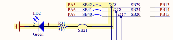
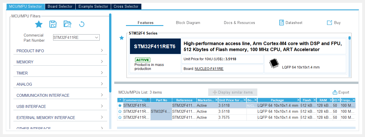
I choose to use a Nucleo-64 board with STM32F411RE.
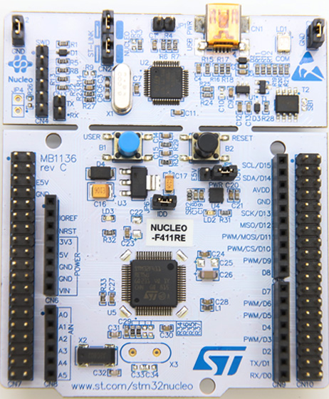
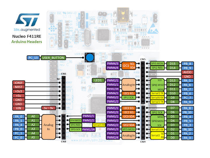
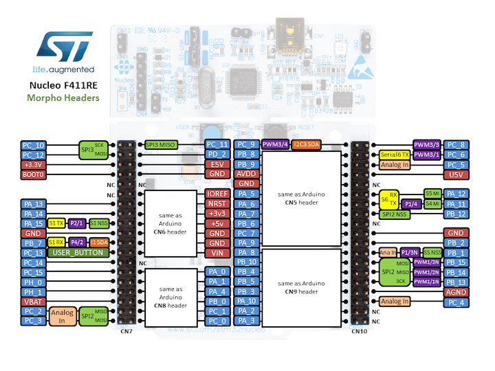
The Green LED is connected to the pin PA5 of the MCU.
Learn through example
Please note that the below examples just do a very simple thing, but ther are explained in details, so it may be quite difficult to follow if you are not familiar to programming MCU at low-level. Let see what we can learn.
Register-based Code Example#
Step 1: Select the Target device#
You can find the target using either MCU Selector or Board Selector.
Step 2: Select Project type#
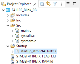
In this example, we do not use any help from the CubeMX, so let choose Empty in project type option.
![]()
The project will be created with minimal number of files. You will see a startup file, some source files for System Calls, Memory Management; however, at this moment, you don’t need to understand them, because most of their content are dummy or default settings.
Step 3: Configure registers#
So, this is a difficult step. You don’t know where to start, do you? Go back to the Documents guide and start reading and find what we want. Read the Reference manual first!!!
Check the Memory Map to know the address of Peripherals:
Table 1. STM32F411xC/E register boundary addresses
Boundary address            Bus         Peripheral
0x40023800 - 0x40023BFF     AHB1        RCC (Clock)
0x40020000 - 0x400203FF     AHB1        GPIOA (I/O)
So, define the base addresses:
#define RCC_BASE        0x40023800UL
#define GPIOA_BASE      0x40020000UL
Configure Clock
Read the register description to know the offset and config value:
6.3.1 Clock control register (RCC_CR)
Address offset:
0x00
Reset value:0x0000XX81
→ HSION is enabled by default. HSI is 16 MHz.
6.3.3 Clock configuration register (RCC_CFGR)
Address offset:
0x08
Reset value:0x00000000
→ HSI oscillator is used as the system clock, no divider activated. System is clocked at 16 MHz (equal to HSI’s Frequency).
The GPIOA is on AHB1 bus, therefore, check the clock on AHB Bus:
6.3.9 AHB peripheral clock enable register (RCC_AHB1ENR)
Address offset:
0x30
Reset value:0x00000000
→ GPIO Clock is disabled by default. Need to enable GPIOAEN bit:
#define RCC_AHB1ENR      RCC_BASE + 0x30
*(uint32_t *)(RCC_AHB1ENR) |= (1 << 0);
Configure GPIO Port and Pin
Read the register description to know the offset and config value:
8 General-purpose I/Os (GPIO)
Each general-purpose I/O port has four 32-bit configuration registers (
GPIOx_MODER,GPIOx_OTYPER,GPIOx_OSPEEDRandGPIOx_PUPDR), two 32-bit data registers (GPIOx_IDRandGPIOx_ODR) and a 32-bit set/reset register (GPIOx_BSRR).8.3.5 I/O data bitwise handling
The bit set reset register (GPIOx_BSRR) is a 32-bit register which allows the application to set and reset each individual bit in the output data register (
GPIOx_ODR).When written to
1, bit BS(i) sets the corresponding ODR(i) bit. When written to1, bit BR(i) resets the ODR(i) corresponding bit.Writing any bit to
0inGPIOx_BSRRdoes not have any effect on the corresponding bit inGPIOx_ODR. If there is an attempt to both set and reset a bit inGPIOx_BSRR, the set action takes priorityUsing the
GPIOx_BSRRregister to change the values of individual bits inGPIOx_ODRis a “one-shot” effect that does not lock theGPIOx_ODRbits.
Do the same reading and understanding as we do with Clock registers, here are what we have to do:
- Set Pin 5 on Port A to Output mode on bit
[11:10]of theGPIOA_MODERregister - To output HIGH value, set bit
5of theGPIOA_BSRRregister - To output LOW value, set bit
21of theGPIOA_BSRRregister
#define GPIOA_MODER     GPIOA_BASE + 0x00
#define GPIOA_BSRR      GPIOA_BASE + 0x18

*(uint32_t *)(GPIOA_MODER)  &= ~(1 << 11);
*(uint32_t *)(GPIOA_MODER)  |=  (1 << 10);
*(uint32_t *)(GPIOA_BSRR)   |=  (1 << (5   ));
*(uint32_t *)(GPIOA_BSRR)   |=  (1 << (5+16));
Delay
We know that MCU is running at 16 MHz (HSI), we can make a loop for delay as below. If each loop needs 10 instruction cycles, to delay 50 ms, the number of iterations is: \(\frac{0.05 \times 16000000}{10} = 80000\)
Note that this is a blocking delay, MCU is only doing the loop.
#define DELAY_MAX 80000;
for(uint32_t i=DELAY_MAX; i--;);
Step 4: The complete code#
You can assemble all above pieces of code in the main.c file.
#include <stdint.h>

/* Register Addresses*/

/* Clock */
#define RCC_BASE        0x40023800UL
#define RCC_AHB1ENR     RCC_BASE + 0x30

/* GPIO */
#define GPIOA_BASE      0x40020000UL
#define GPIOA_MODER     GPIOA_BASE + 0x00
#define GPIOA_BSRR      GPIOA_BASE + 0x18

/* delay counter */
#define DELAY_MAX       50000

int main(void)
{
  /* turn on clock on GPIOA */
  *(uint32_t *)(RCC_AHB1ENR) |= (1 << 0);

  /* set PA5 to output mode */
  *(uint32_t *)(GPIOA_MODER)  &= ~(1 << 11);
  *(uint32_t *)(GPIOA_MODER)  |=  (1 << 10);

  while(1) {
    /* set HIGH value on pin PA5 */
    *(uint32_t *)(GPIOA_BSRR)   |=  (1 <<  5);
    for(uint32_t i=DELAY_MAX; i--;);

    /* set LOW value on pin PA5 */
    *(uint32_t *)(GPIOA_BSRR)    |=  (1 << (5+16));
    for(uint32_t i=DELAY_MAX; i--;);
  }
}
Step 5: Check the compilation settings#
There are some setting groups we need to check, right-click on the Project and select Properties:
- Paths and Symbols
-
- Includes are the directories to find headers, note that there is no extra included folder
- Symbols are extra definitions enable/disable some blocks of code. Note the symbol
STM32,STM32F4and the target MCUSTM32F411RETxare added automatically. For debug session, the symbolDEBUGis added too. - Source Location are the directories containing source code which is going to be compiled
- Compilation Settings
-
-
MCU Settings:
- the Floating Point Unit =
FPv4-SP-D16; use-mfloat-abi=hard - the library for C is Reduced C
--specs=nano.specs
- the Floating Point Unit =
-
GCC Assembler: Target specs, including CPU, Debug
- Inline assembler:
-x assembler-with-cpp - Target specs:
-mcpu=cortex-m4 -mthumb -mfpu=fpv4-sp-d16 -mfloat-abi=hard - Library specs:
--specs=nano.specs - Debug level:
-DDEBUG -g3
- Inline assembler:
-
GCC Compiler:
- C language standard:
-std=gnu11 - Target specs:
-mcpu=cortex-m4 -mthumb -mfpu=fpv4-sp-d16 -mfloat-abi=hard - Library specs:
--specs=nano.specs - Debug level:
-DDEBUG -g3 - Preprocessor:
-DSTM32 -DSTM32F4 -DSTM32F411RETx - Include paths:
-I <paths> - Optimization: No optimization
-O0, but place functions and data in separated sections for clean up dead code-ffunction-sections -fdata-sections - Warning:
-Wall - Stack Usage analysis:
-fstack-usage
- C language standard:
-
GCC Linker:
- Target specs:
-mcpu=cortex-m4 -mthumb -mfpu=fpv4-sp-d16 -mfloat-abi=hard - Library specs:
--specs=nano.specs - System call: Minimal implementation
--specs=nosys.specs - Generate Map file:
-Wl,-Map={file} - Clean up unused sections:
-Wl,--gc-sections - Linker file:
-T"<file>" - Library:
-lc -lm, these libraries will be search in a loop to check forward declaration and cross-dependency, so they are inside the marks-Wl,--start-groupand-Wl,--end-group
- Target specs:
-
Step 6: Check build output#
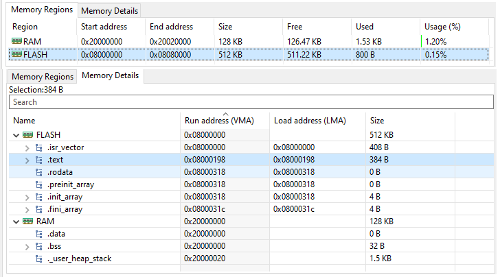
Just only Blink a LED, the resource usage is about 800 B of Flash, 32 B allocated on RAM
Step 7: Run on board#
Select Run and choose the target board to run. At this moment, just use default configuration for a Debug session.
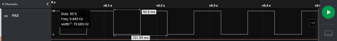
Hook a Logic Analyzer to check the output waveform:
Low-Level CMSIS Code Example#
Step 1: Select the Target device#
Same as Register-based Code Example: Use STM32F411RETx.
Step 2: Select the target Firmware Package#
Same as Register-based Code Example: Use C Language in an Empty Project.
Step 3: Integrate CMSIS Pack#
The Common Microcontroller Software Interface Standard (CMSIS) is a vendor-independent abstraction layer for microcontrollers that are based on Arm Cortex processors. CMSIS defines generic tool interfaces and enables consistent device support. This layer is adopted by leading semiconductor companies, embedded software and tools vendors across the Arm architecture. This means you can find a CMSIS-Pack for your target MCU if the MCU’s vendor is registered with ARM.
Integrate the CMSIS to your project:
-
Download CMSIS Core, the latest version is CMSIS 5.
The filename, for example, isARM.CMSIS.5.8.0.pack, you can unzip it as a normal zip file. -
Copy the header files in
ARM.CMSIS.5.8.0.pack/CMSIS/Core/Includeto your project -
Download CMSIS-Pack for the target MCU:
-
Select STMicroelectronics → STM32F4 Series → STM32F411 → STM32F41RE → STM32F411RETx
-
Download the STM32F4 Device Support Package (DSP). Filename is
Keil.STM32F4xx_DFP.2.16.0.pack, for example. You can unzip it as a zip file.
-
-
Copy the header files in
Keil.STM32F4xx_DFP.2.16.0.pack/Drivers/CMSIS/Device/ST/STM32F4xx/Includeto your project -
Add header paths to project by opening adding
CMSIS/Core/IncludeandCMSIS/Device/ST/STM32F4xx/Includeto project Paths and Symbols: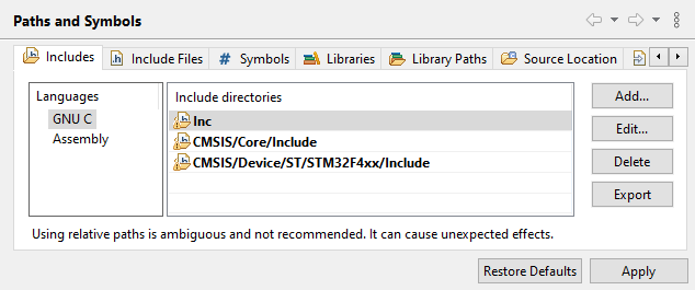
Include CMSIS and STMF4xx headers -
Add a symbol
STM32F411xEto enable target inclusion in the general header filestm32f4xx.h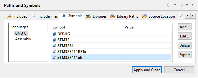
Add STM32F411xEsymbol -
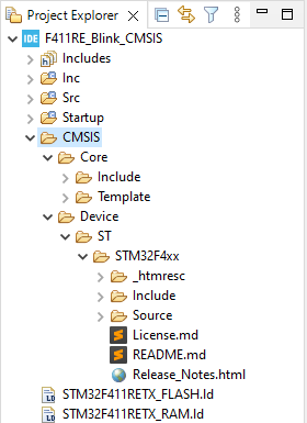
Add
system_stm32f4xx.cto project source code, as this file implementsSystemInit()andSystemCoreClockUpdate()
Only add system_stm32f4xx.cand ignore all other templates -
Include the header file of the target device, such as:
#include <stm32f4xx.h>
Register-based
CMSIS
Step 4: Use defined registers#
Follow the same rule of reading the Reference Manual document which can be found in the Keil.STM32F4xx_DFP.2.16.0/Documentation folder, you will have to do the same steps of configuring clocks, GPIO. However, this time, you can use the definitions and macros written in the device header files. All registers name listed in the Reference Manual document are available to use.
Configure Clock
Use the RCC peripheral, set the bit RCC_AHB1ENR_GPIOAEN in the AHB1ENR register to enable clock for GPIOA.
RCC->AHB1ENR |= RCC_AHB1ENR_GPIOAEN;
Configure GPIOA
Use the GPIOA peripheral, set the field MODER8 to 01 in the register MODER to set pin PA5 as output.
GPIOA->MODER &= ~GPIO_MODER_MODER8_1;
GPIOA->MODER |=  GPIO_MODER_MODER8_0;
To set HIGH value, set the bit GPIO_BSRR_BS_5 on the BSRR register. To clear the value, set the bit GPIO_BSRR_BR_5 on the BSRR register.
GPIOA->BSRR |= GPIO_BSRR_BS_5;
GPIOA->BSRR |= GPIO_BSRR_BR_5;
That’s it! Very simple and easy to understand the source code.
Step 5: The completed code#
You can assemble all above pieces of code in the main.c file.
#include <stdint.h>
#include <stm32f4xx.h>

/* delay counter */
#define DELAY_MAX       50000

int main(void)
{
  /* turn on clock on GPIOA */
  RCC->AHB1ENR |= RCC_AHB1ENR_GPIOAEN;

  /* set PA5 to output mode */
  GPIOA->MODER &= ~GPIO_MODER_MODE5_1;
  GPIOA->MODER |=  GPIO_MODER_MODE5_0;

  while(1) {
      /* set HIGH value on pin PA5 */
      GPIOA->BSRR |= GPIO_BSRR_BS_5;
      for(uint32_t i=DELAY_MAX; i--;);

      /* set LOW value on pin PA5 */
      GPIOA->BSRR |= GPIO_BSRR_BR_5;
      for(uint32_t i=DELAY_MAX; i--;);
    }
}
Register-based
/* turn on clock on GPIOA */
*(uint32_t *)(RCC_AHB1ENR) |= (1 << 0);
Register-based CMSIS
/* turn on clock on GPIOA */
RCC->AHB1ENR |= RCC_AHB1ENR_GPIOAEN;
/* set GPIOA to output mode */
*(uint32_t *)(GPIOA_MODER)  &= ~(1 << 11);
*(uint32_t *)(GPIOA_MODER)  |=  (1 << 10);
/* set GPIOA to output mode */
GPIOA->MODER &= ~GPIO_MODER_MODE5_1;
GPIOA->MODER |=  GPIO_MODER_MODE5_0;
while(1) {
    /* set HIGH value on pin PA5 */
    *(uint32_t *)(GPIOA_BSRR) |=  (1 <<  5);
    for(uint32_t i=DELAY_MAX; i--;);

    /* set LOW value on pin PA5 */
    *(uint32_t *)(GPIOA_BSRR) |=  (1 << (5+16));
    for(uint32_t i=DELAY_MAX; i--;);
}
while(1) {
    /* set HIGH value on pin PA5 */
    GPIOA->BSRR |= GPIO_BSRR_BS_5;
    for(uint32_t i=DELAY_MAX; i--;);

    /* set LOW value on pin PA5 */
    GPIOA->BSRR |= GPIO_BSRR_BR_5;
    for(uint32_t i=DELAY_MAX; i--;);
}
Step 6: Check the compilation settings#
There are some setting groups we need to check, right-click on the Project and select Properties:
- Paths and Symbols
-
- Includes are the directories to find headers, note that there is no extra included folder
- Symbols are extra definitions enable/disable some block of code. Note the symbol
STM32,STM32F4and the target MCUSTM32F411RETxare added automatically. To use the header filestm32f4xx.h, you must add the definitionSTM32F411xEin the Project Symbols. - Source Location are the directories containing source code which is going to be compiled
- Compilation Settings
- The same as the Register-based Code Example.
Step 7: Check build output#
Just only Blink a LED, the resource usage is the same as the Register-base Code Example, as we still access directly to register using their names.
Step 8: Run on board#
Select Run and choose the target board to run. At this moment, just use default configuration for a Debug session.
Low-Level Generated Code Example#
Step 1: Select the Target device#
Same as Register-based Code Example: Use STM32F411RETx.
Step 2: Select the target Firmware Package#
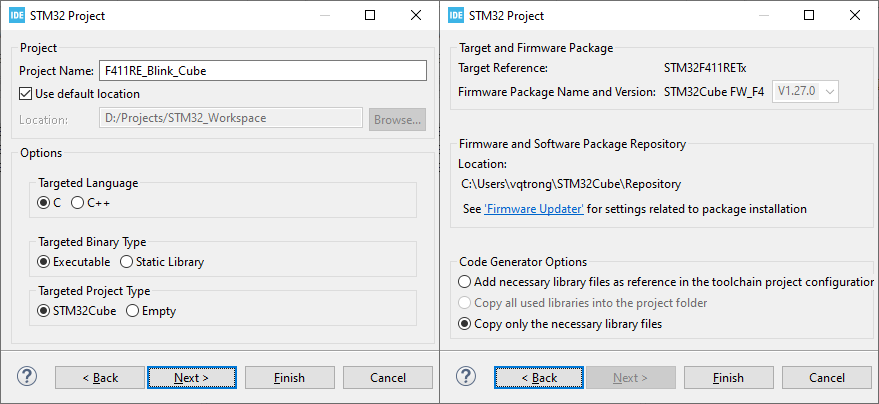
You have to choose a name for your project.
Then select STM32Cube as the targeted type, and then use a targeted Firmware Package.
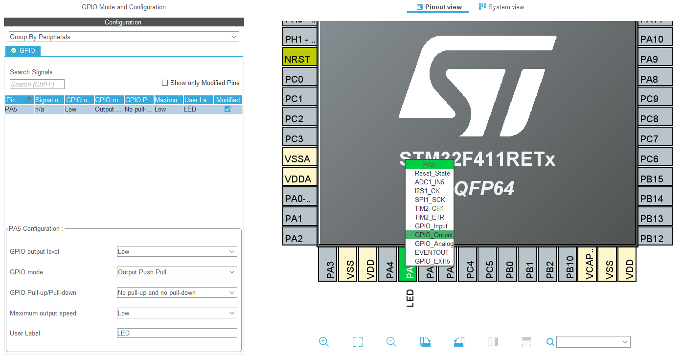
Step 3: Assign the LED pin#
In the Pinout & Configuration tab:
- Click on the pin
PA5and selectGPIO Output - Change its name to
LEDusing the right click.
Under the GPIO Configuration panel, take note the default settings for PA5:
- GPIO Output Level:
Low, this pin is at Low level at startup - GPIO Mode:
Output Push-Pull, this pin is kept connected to the driven signal, read more in GPIO Output Modes - GPIO Pull-up/Pull-down:
No Pull, because in Output Push-Pull mode, internal resistor does not take effect. Only in Output Open-Drain mode, Pull-Up resister can help to drive the pin at High level - Max Output Speed:
Low, this is crew rate meaning how fast the signal can change its level - User label:
LED, a name to use instead of the pin name PA5
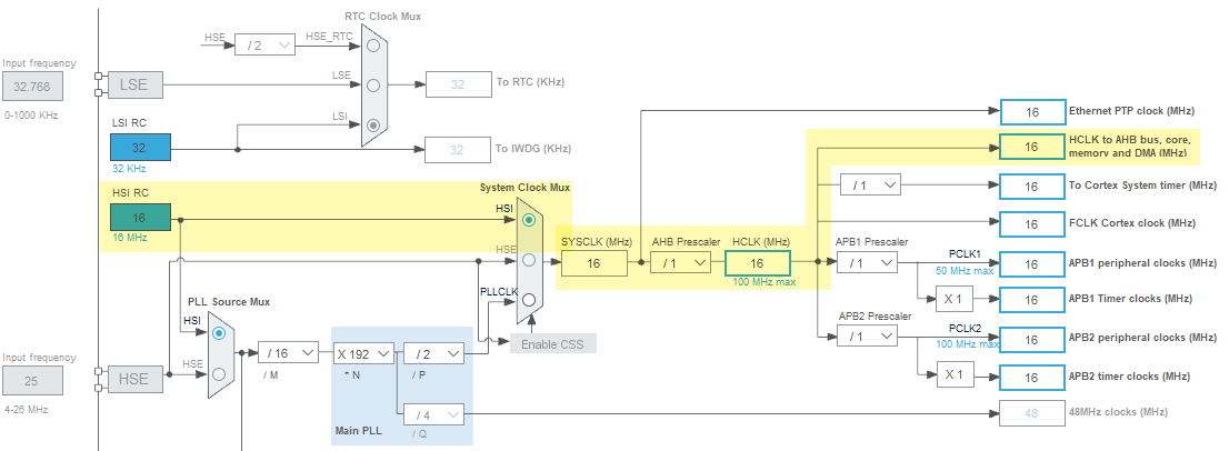
Step 4: Select Clock paths#
In the Clock Configuration, check the default settings for the Clock:
- System Clock Mux:
HSI, this is high-speed internal clock at 8 MHz - All prescaler:
1, there is no modification on clock line, therefore, the core and all peripherals use the SYSCLK at 16 MHz
Step 5: Select LL firmware packages#
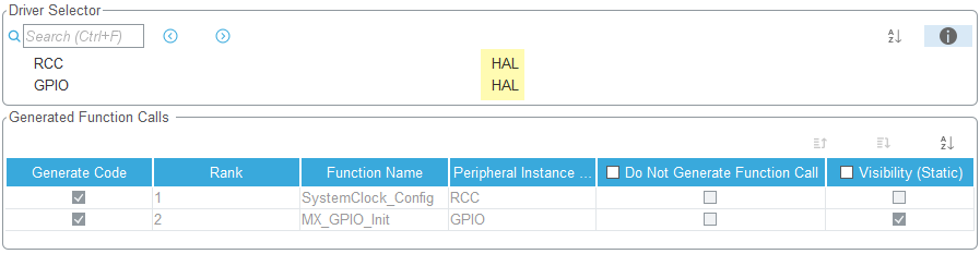
In the Project Manager, under the Advanced Settings, make sure Driver Selector is LL for RCC (Clock Configs) and GPIO (Pin Output).
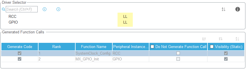
Step 6: Generate LL Code#
Press Alt+K or click on menu Project → Generate Code.
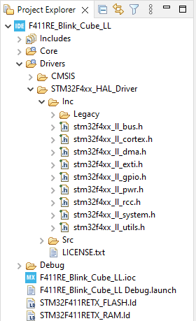
The STM32F4xx_HAL_Driver with LL source code and the CMSIS driver are copied to the project folder.
CMSIS
Low-Level
The Clock Configs:
CMSIS
/* turn on clock on GPIOA */
RCC->AHB1ENR |= RCC_AHB1ENR_GPIOAEN;
Low-Level
void SystemClock_Config(void) {
  LL_FLASH_SetLatency(LL_FLASH_LATENCY_0);
  while(LL_FLASH_GetLatency()
    != LL_FLASH_LATENCY_0
  ){}

  LL_PWR_SetRegulVoltageScaling(
      LL_PWR_REGU_VOLTAGE_SCALE1
  );
  LL_RCC_HSI_SetCalibTrimming(16);
  LL_RCC_HSI_Enable();

  /* Wait till HSI is ready */
  while(LL_RCC_HSI_IsReady() != 1){}

  LL_RCC_SetAHBPrescaler(LL_RCC_SYSCLK_DIV_1);
  LL_RCC_SetAPB1Prescaler(LL_RCC_APB1_DIV_1);
  LL_RCC_SetAPB2Prescaler(LL_RCC_APB2_DIV_1);
  LL_RCC_SetSysClkSource(
    LL_RCC_SYS_CLKSOURCE_HSI
  );

  /* Wait till System clock is ready */
  while(LL_RCC_GetSysClkSource()
    != LL_RCC_SYS_CLKSOURCE_STATUS_HSI
  ){}

  LL_Init1msTick(16000000);
  LL_SetSystemCoreClock(16000000);
  LL_RCC_SetTIMPrescaler(
    LL_RCC_TIM_PRESCALER_TWICE
  );
}
The GPIO Configs:
CMSIS
/* set GPIOA to output mode */
GPIOA->MODER &= ~GPIO_MODER_MODE5_1;
GPIOA->MODER |=  GPIO_MODER_MODE5_0;
Low-Level
static void MX_GPIO_Init(void) {
  LL_GPIO_InitTypeDef GPIO_InitStruct = {0};

  /* GPIO Ports Clock Enable */
  LL_AHB1_GRP1_EnableClock(
      LL_AHB1_GRP1_PERIPH_GPIOA
  );

  /**/
  LL_GPIO_ResetOutputPin(
    LED_GPIO_Port, LED_Pin
  );

  /**/
  GPIO_InitStruct.Pin = LED_Pin;
  GPIO_InitStruct.Mode = LL_GPIO_MODE_OUTPUT;
  GPIO_InitStruct.Speed =
    LL_GPIO_SPEED_FREQ_LOW;
  GPIO_InitStruct.OutputType =
    LL_GPIO_OUTPUT_PUSHPULL;
  GPIO_InitStruct.Pull =
    LL_GPIO_PULL_NO;
  LL_GPIO_Init(
    LED_GPIO_Port, &GPIO_InitStruct
  );
}
Step 7: Blink LED using LL APIs#
The low-layer (LL) drivers are designed to offer a fast light-weight expert-oriented layer which is closer to the hardware.
For the GPIO module, you should read the document UM1725 - Description of STM32F4 HAL and low-layer drivers, you will find an instruction:
To set/reset the level of a pin configured in output mode use
LL_GPIO_SetOutputPin()orLL_GPIO_ResetOutputPin()
Now, blink the LED in the main while loop, note that, we also have a delay function LL_mDelay().
CMSIS
while (1) {
    /* set HIGH value on pin PA5 */
    GPIOA->BSRR |= GPIO_BSRR_BS_5;
    for(uint32_t i=DELAY_MAX; i--;);

    /* set LOW value on pin PA5 */
    GPIOA->BSRR |= GPIO_BSRR_BR_5;
    for(uint32_t i=DELAY_MAX; i--;);
}
Low-Level
while (1) {
    LL_GPIO_SetOutputPin(
        LED_GPIO_Port, LED_Pin
    );
    LL_mDelay(DELAY_MAX);

    LL_GPIO_ResetOutputPin(
        LED_GPIO_Port, LED_Pin
    );
    LL_mDelay(DELAY_MAX);
}
Step 8: Check the compilation settings#
There are some setting groups we need to check, right-click on the Project and select Properties:
- Paths and Symbols
-
- Includes are the directories to find headers, note the
STM32F4xx_HAL_DriverandCMSIS - Symbols are extra definitions enable/disable some block of code. Note the symbol
USE_FULL_LL_DRIVERand the target MCUSTM32F411xEThere are also many other definitions such asHSI_VALUEHSE_VALUEfor clock settings;DATA_CACHE_ENABLE,INSTRUCTION_CACHE_ENABLE,PREFETCH_ENABLEfor pipeline settings; - Source Location are the directories containing source code which is going to be compiled
- Includes are the directories to find headers, note the
- Compilation Settings
- Same as the Register-based Code Example.
Step 9: Check build output#
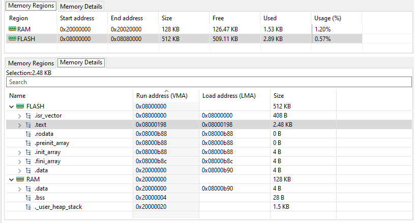
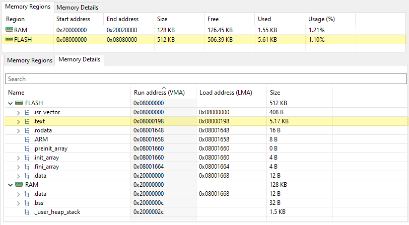
Just only Blink a LED, the resource usage more than 3 times of Registered-based example, as it uses 2.48 KB of Flash.
Step 10: Run on board#
Select Run and choose the target board to run. At this moment, just use default configuration for a Debug session.
High-level Generated Code#
Step 1: Select the Target device#
Same as Low-Level Generated Code Example: Use STM32F411RETx.
Step 2: Select the target Firmware Package#
Same as Low-Level Generated Code Example: Use C Language in a STM32Cube Project.
Step 3: Assign the LED pin#
Same as Low-Level Generated Code Example: Set pin PA5 to GPIO_Output and name it LED.
Step 4: Select Clock paths#
Same as Low-Level Generated Code Example: Leave every in default state to select HSI at 16 MHz.
Step 5: Select HAL firmware package#
In the Project Manager, under the Advanced Settings, make sure Driver Selector is HAL for RCC (Clock Configs) and GPIO (Pin Output).
Step 6: Generate HAL Code#
Press Alt+K or click on menu Project → Generate Code.
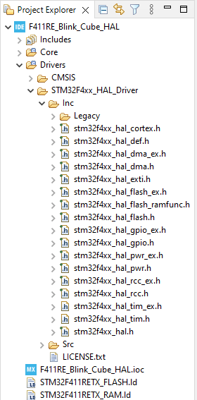
The STM32F4xx_HAL_Driver with HAL source code and the CMSIS driver are copied to the project folder.
Low-Level
HAL
The Clock Configs:
Low-Level
void SystemClock_Config(void) {
    LL_FLASH_SetLatency(LL_FLASH_LATENCY_0);
    while(LL_FLASH_GetLatency()
        != LL_FLASH_LATENCY_0
    ){}

    LL_PWR_SetRegulVoltageScaling(
        LL_PWR_REGU_VOLTAGE_SCALE1
    );
    LL_RCC_HSI_SetCalibTrimming(16);
    LL_RCC_HSI_Enable();

    /* Wait till HSI is ready */
    while(LL_RCC_HSI_IsReady() != 1){}

    LL_RCC_SetAHBPrescaler(LL_RCC_SYSCLK_DIV_1);
    LL_RCC_SetAPB1Prescaler(LL_RCC_APB1_DIV_1);
    LL_RCC_SetAPB2Prescaler(LL_RCC_APB2_DIV_1);
    LL_RCC_SetSysClkSource(
        LL_RCC_SYS_CLKSOURCE_HSI
    );

    /* Wait till System clock is ready */
    while(LL_RCC_GetSysClkSource()
        != LL_RCC_SYS_CLKSOURCE_STATUS_HSI
    ){}

    LL_Init1msTick(16000000);
    LL_SetSystemCoreClock(16000000);
    LL_RCC_SetTIMPrescaler(
        LL_RCC_TIM_PRESCALER_TWICE
    );
}
HAL
void SystemClock_Config(void) {
    RCC_OscInitTypeDef RCC_OscInitStruct = {0};
    RCC_ClkInitTypeDef RCC_ClkInitStruct = {0};

    __HAL_RCC_PWR_CLK_ENABLE();
    __HAL_PWR_VOLTAGESCALING_CONFIG(
        PWR_REGULATOR_VOLTAGE_SCALE1
    );

    RCC_OscInitStruct.OscillatorType =
        RCC_OSCILLATORTYPE_HSI;
    RCC_OscInitStruct.HSIState = RCC_HSI_ON;
    RCC_OscInitStruct.HSICalibrationValue =
        RCC_HSICALIBRATION_DEFAULT;
    RCC_OscInitStruct.PLL.PLLState =
        RCC_PLL_NONE;
    if (HAL_RCC_OscConfig(&RCC_OscInitStruct)
        != HAL_OK
    ){
        Error_Handler();
    }

    RCC_ClkInitStruct.ClockType =
        RCC_CLOCKTYPE_HCLK |
        RCC_CLOCKTYPE_SYSCLK |
        RCC_CLOCKTYPE_PCLK1 |
        RCC_CLOCKTYPE_PCLK2;
    RCC_ClkInitStruct.SYSCLKSource =
        RCC_SYSCLKSOURCE_HSI;
    RCC_ClkInitStruct.AHBCLKDivider =
        RCC_SYSCLK_DIV1;
    RCC_ClkInitStruct.APB1CLKDivider =
        RCC_HCLK_DIV1;
    RCC_ClkInitStruct.APB2CLKDivider =
        RCC_HCLK_DIV1;

    if (HAL_RCC_ClockConfig(
            &RCC_ClkInitStruct, FLASH_LATENCY_0
        ) != HAL_OK
    ){
        Error_Handler();
    }
}
The GPIO Configs:
Low-Level
static void MX_GPIO_Init(void) {
    LL_GPIO_InitTypeDef GPIO_InitStruct = {0};

    /* GPIO Ports Clock Enable */
    LL_AHB1_GRP1_EnableClock(
        LL_AHB1_GRP1_PERIPH_GPIOA
    );

    /**/
    LL_GPIO_ResetOutputPin(
        LED_GPIO_Port, LED_Pin
    );

    /**/
    GPIO_InitStruct.Pin = LED_Pin;
    GPIO_InitStruct.Mode = LL_GPIO_MODE_OUTPUT;
    GPIO_InitStruct.Speed =
        LL_GPIO_SPEED_FREQ_LOW;
    GPIO_InitStruct.OutputType =
        LL_GPIO_OUTPUT_PUSHPULL;
    GPIO_InitStruct.Pull =
        LL_GPIO_PULL_NO;
    LL_GPIO_Init(
        LED_GPIO_Port, &GPIO_InitStruct
    );
}
HAL
static void MX_GPIO_Init(void) {
    GPIO_InitTypeDef GPIO_InitStruct = {0};

    /* GPIO Ports Clock Enable */
    __HAL_RCC_GPIOA_CLK_ENABLE();

    /*Configure GPIO pin Output Level */
    HAL_GPIO_WritePin(
        LED_GPIO_Port, LED_Pin, GPIO_PIN_RESET
    );

    /*Configure GPIO pin : LED_Pin */
    GPIO_InitStruct.Pin = LED_Pin;
    GPIO_InitStruct.Mode = GPIO_MODE_OUTPUT_PP;
    GPIO_InitStruct.Pull = GPIO_NOPULL;
    GPIO_InitStruct.Speed = GPIO_SPEED_FREQ_LOW;

    HAL_GPIO_Init(
        LED_GPIO_Port, &GPIO_InitStruct
    );
}
Step 7: Blink LED using HAL API#
The Hardware Abstract Layer (HAL) is designed so that it abstracts from the specific peripheral memory mapping. But, it also provides a general and more user-friendly way to configure the peripheral, without forcing the programmers to now how to configure its registers in detail.
For the GPIO module, you should read the document Description of STM32F4 HAL and low-layer drivers, you will find an instruction:
To set/reset the level of a pin configured in output mode use
HAL_GPIO_WritePin()orHAL_GPIO_TogglePin()
Now, blink the LED in the main while loop, note that, we also have a delay function HAL_Delay().
Low-Level
while (1) {
    LL_GPIO_SetOutputPin(
        LED_GPIO_Port, LED_Pin
    );
    LL_mDelay(DELAY_MAX);

    LL_GPIO_ResetOutputPin(
        LED_GPIO_Port, LED_Pin
    );
    LL_mDelay(DELAY_MAX);
}
HAL
while(1) {
    HAL_GPIO_WritePin(
        LED_GPIO_Port, LED_Pin, GPIO_PIN_SET
    );
    HAL_Delay(DELAY_MAX);

    HAL_GPIO_WritePin(
        LED_GPIO_Port, LED_Pin, GPIO_PIN_RESET
    );
    HAL_Delay(DELAY_MAX);
}
Step 8: Check the compilation settings#
There are some setting groups we need to check, right-click on the Project and select Properties:
- Paths and Symbols
-
- Includes are the directories to find headers, note the
STM32F4xx_HAL_DriverandCMSIS - Symbols are extra definitions enable/disable some block of code. Note the symbol
USE_HAL_DRIVERand the target MCUSTM32F411xE - Source Location are the directories containing source code which is going to be compiled
- Includes are the directories to find headers, note the
- Compilation Settings
- Same as the Low-Level Generated Code Example.
Step 9: Check build output#
Just only Blink a LED, the resource usage is twice of the Low-level case, and 6 times of the Register-based case.
Step 10: Run on board#
Select Run and choose the target board to run. At this moment, just use default configuration for a Debug session.